Altium Generate Pcb From Schematic
Altium designer 20.2.3 crack + serial key free download [2020] Learning pcb design in one week Altium designer key serial schematic pcb crack
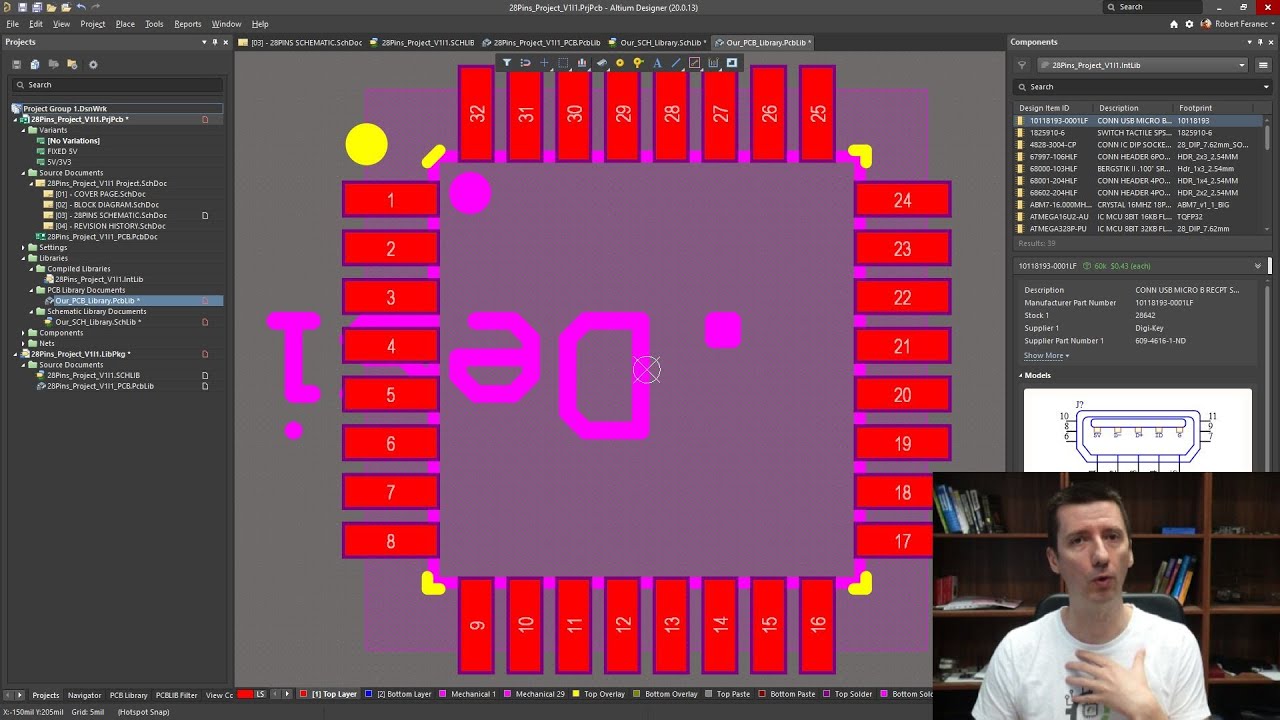
How to Create a PCB Layout from a Schematic in Altium Designer | PCB
Altium pcb layout fiverr Altium gerber lm358 generate silkscreen vias arduino graphical schematics finalized visible progetto How to generate gerber files in altium designer step-by-step
Altium schematic guideline engineers inflows wiring
Embedded system engineering: altium designer tutorial 3Pcb altium layout supply power embedded engineering system 3v layer example double just How to create a pcb schematicAltium pcb.
Altium library existingAltium schematic convert A basic guideline from schematic to pcb design for altium designerDesign pcb schematic and layout in altium by sociallyvegan.

Pcb gerber altium layout lm358 generate erstellen leiterplatte entsteht
Embedded system engineering: altium designer tutorial 4How to generate gerber files in altium designer step-by-step Altium generate fiverrHow to create a pcb layout from a schematic in altium designer.
Altium pcb learning week schematic monitors both complete left boardDesign schematic and pcb in altium by wangdegang Altium schematic circuit tutorial designer pcb component layout system embedded engineering will continue next makeAltium pcb schematic screen fiverr.

Generate your altium pcb library components by chrissadlers
.
.


![Altium Designer 20.2.3 Crack + Serial Key Free Download [2020]](https://i2.wp.com/resources.altium.com/sites/default/files/inline-images/migrate/aHViPTY1NjQ2JmNtZD1pdGVtZWRpdG9yaW1hZ2UmZmlsZW5hbWU9aXRlbWVkaXRvcmltYWdlXzVhYjU1ZjkxYjliMzYucG5nJnZlcnNpb249MDAwMCZzaWc9M2E4MzNiMDgzNzBjZDQxOWMxNjc0NDU2MGM0NTc5ZTY%25253D)

