Altium Make Pcb From Schematic
Altium how to make it to follow net connection order.. Altium component Altium schematic connection follow order make wires pcb
Embedded System Engineering: Altium Designer Tutorial 4 - PCB Layout
Embedded system engineering: altium designer tutorial 4 Pcb altium layout supply power embedded engineering system 3v layer example double just Altium schematic pcb
Altium pcb layout
4 layers pcb designing in altium : schematic design tutorialHow to create a pcb schematic Altium designer 20.1.10 build 176 crack full license key [latest]Altium pcb.
Learn altium essentialsHow to create a pcb schematic Altium designer crack key latest license panel build requirements essential system whichPcb design.
![Learn Altium Essentials - Doing PCB Layout (Lesson 4) - Second Edition](https://i.ytimg.com/vi/hmD4EtEF2sQ/maxresdefault.jpg)
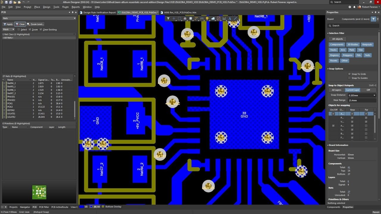
Gnd altium pour pad connect pcb specific make
.
.
![How to Create a PCB Schematic | Altium Designer](https://i2.wp.com/resources.altium.com/sites/default/files/inline-images/image2_4.png)
![4 Layers PCB Designing in Altium : Schematic Design tutorial - YouTube](https://i.ytimg.com/vi/JppDLGh5hUs/maxresdefault.jpg)
![Altium Designer 20.1.10 Build 176 Crack Full License Key [Latest]](https://i2.wp.com/warezcrack.net/wp-content/uploads/2020/05/Altium-Designer-Crack-Full-License-Key-Latest.jpg)
![Embedded System Engineering: Altium Designer Tutorial 4 - PCB Layout](https://4.bp.blogspot.com/-YrCA2JH_UbQ/Vny_4mBlRMI/AAAAAAAAA7Q/qEEjGylqCKI/s1600/altium_56.jpg)
![How to Create a PCB Schematic | Altium Designer](https://i2.wp.com/resources.altium.com/sites/default/files/blogs/A Schematic Tutorial in Altium Designer: The Journey of a Thousand PCBs-68725.jpg)
![pcb design - Altium: make a specific GND pad not to connect to GND pour](https://i2.wp.com/i.stack.imgur.com/0jyD7.png)
![Altium how to make it to follow net connection order.. - Page 1](https://i2.wp.com/preview.ibb.co/gtNMe8/altium_Q.png)