Altium Place Component From Schematic To Pcb
Altium tutorial 12-how to measure distance between components,place Altium schematic pcb Altium components schaltplan shortcuts composants bauteile markierten counterparts pcb
How to Create a PCB Schematic | Altium Designer
Learning pcb design in one week 14. tutorial update schematic component from other library altium Altium designer crack key latest license panel build requirements essential system which
Design schematics and pcb for you in altium designer by ahtishamkhan888
Pcb components altium generated documents same update placeAltium session intent verification hierarchy essentials schematics hierarchical sessions Place componentDesign schematic and pcb in altium by wangdegang.
Altium fiverrAltium schematic component Altium schematic lm386Embedded system engineering: altium designer tutorial 4.
![Altium Designer 20.1.10 Build 176 Crack Full License Key [Latest]](https://i2.wp.com/warezcrack.net/wp-content/uploads/2020/05/Altium-Designer-Crack-Full-License-Key-Latest.jpg)
Altium pcb schematic screen fiverr
How do i flip and rotate components in altium designerAltium schematic convert Component altium place4 layers pcb designing in altium : schematic design tutorial.
Altium designer 20.1.10 build 176 crack full license key [latest]Altium designer basic tutorial Altium pcb schematicsAltium pcb learning week schematic monitors both complete left board.

Altium component pcb adding custom
Part placement shortcuts in altium designerDesign pcb schematic and layout in altium by sociallyvegan Altium adding custom component to pcbAltium schematics schematic fiverr.
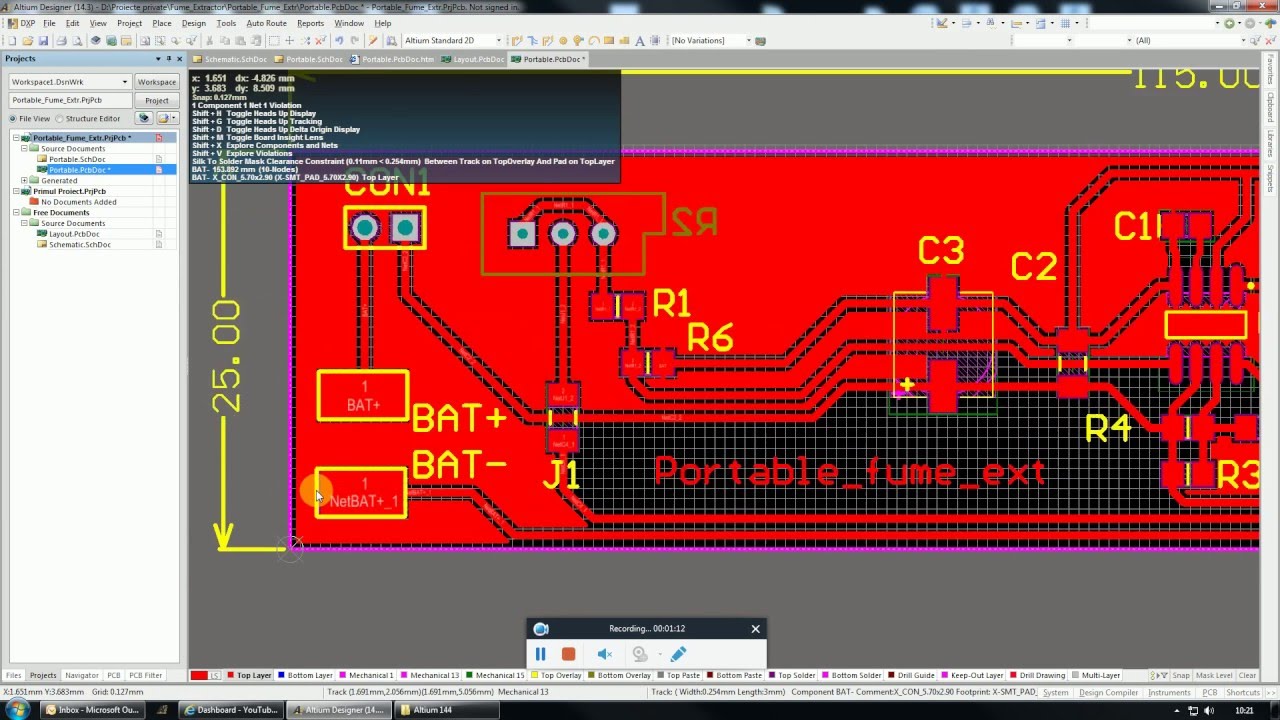
Altium pcb 350m compressionAltium academy virtual session: essentials Altium component library downloadAltium "update pcb documents", components are generated at the same.

Altium pcb designer tutorial example component embedded engineering system position move location place them right
Altium rotate placing functionsHow to create a pcb layout from a schematic in altium designer Altium pcb components distance between measure dimensionsHow to create a pcb schematic.
.