Altium Schematic Page Size
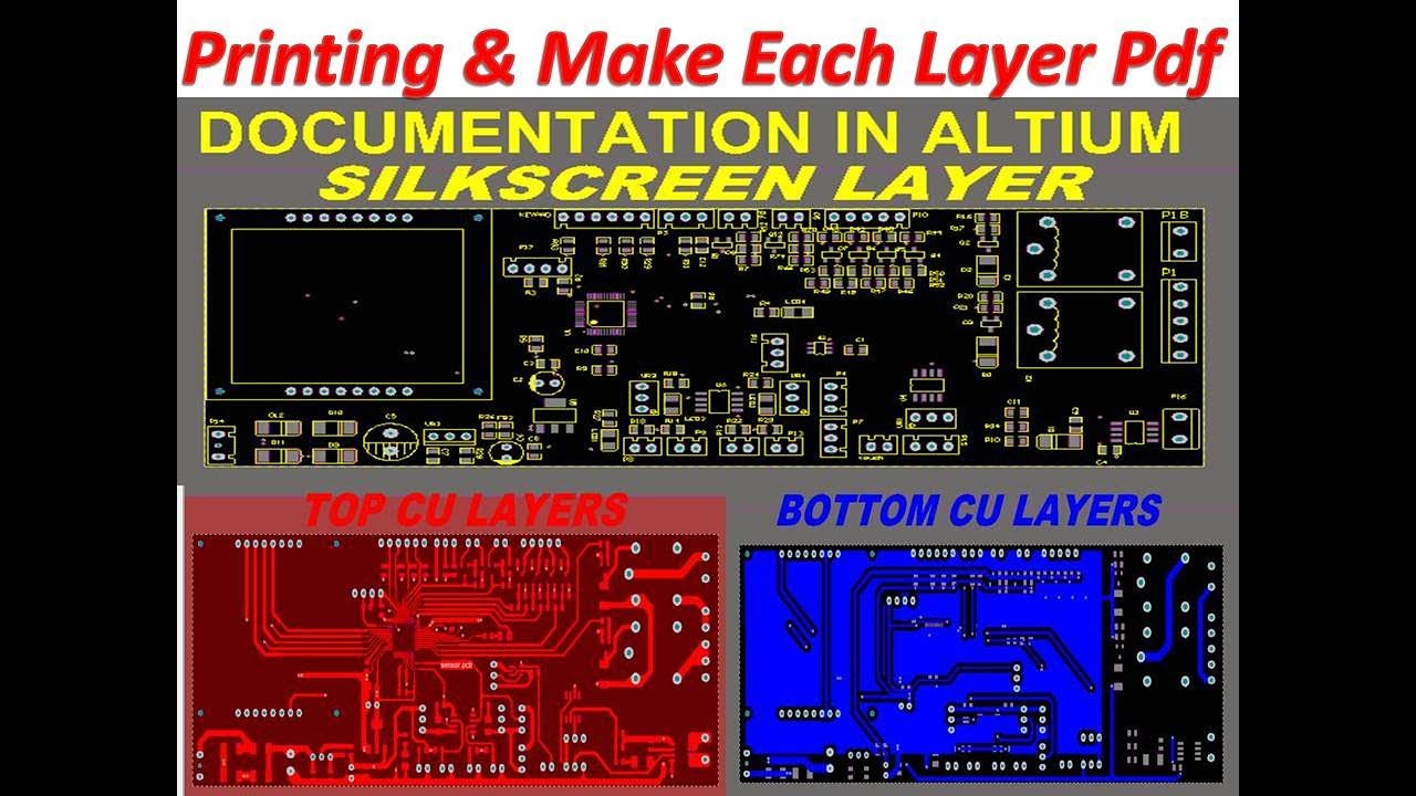
Create a custom altium schematic template Altium tutorial-21: how to print exact size layout layers Sheet size altium electrical designer set a4
4 Layers PCB Designing in Altium : Schematic Design tutorial - YouTube
Altium trace designer spacing minimum identifying nets selecting class pcb width using Schematic altium mismatch pdk ops document between devzone specification sheet nordic Identifying minimum pcb trace spacing and width in altium designer
Template schematic altium create custom pcb 3d
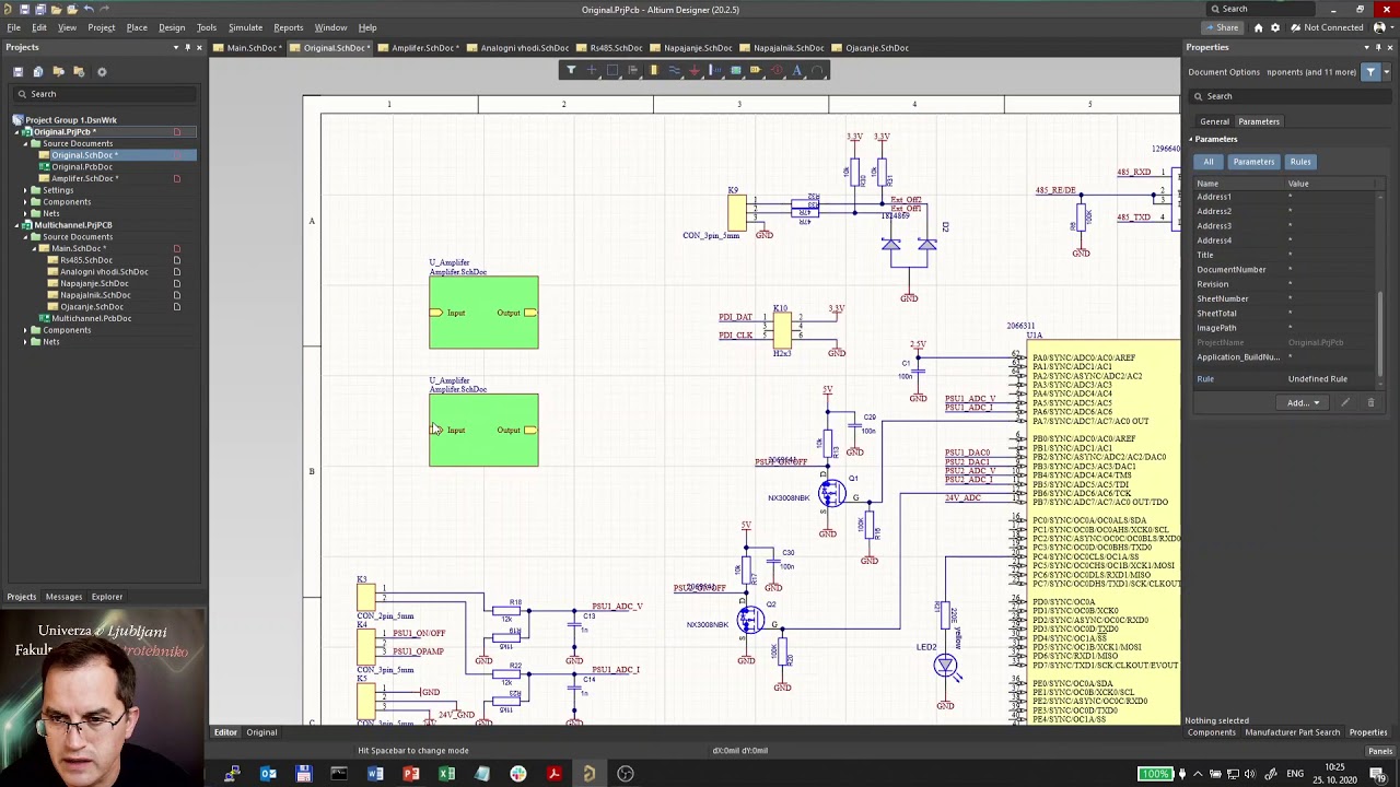
Altium designer getting started user guide & video tutorialsStart your schematic with generic components Altium schematic toplevel digitizer repeated eevblog times forumAltium library schematic.
Altium schematicHow to set the sheet size in altium designer? Altium schematics #01: hierarchical schematics designAltium generic schematic.

Altium print
Altium designer compile sheet error schematics label problem there whenPcb design course Altium schematic previewAltium hierarchical.
Schematic mismatch between ops document and pdk schematicCreating and modifying components in altium schematics Altium basic schematic developmentAltium schematic hackaday io amplifier.

Altium schematic pcb
[solved, i think] altium, differential signals, harnesses and net4 layers pcb designing in altium : schematic design tutorial .
.
![[solved, I think] Altium, Differential Signals, Harnesses and Net](https://i2.wp.com/i.imgur.com/dMwvJi6.png)