Demonstrate Stuck-at-faults In 6t Sram Cell
The leakage power of 6t and 9t sram cells in the standby mode A simple 6t sram cell. the cell is biased toward the 1-state by Sram transistor sizing 6t
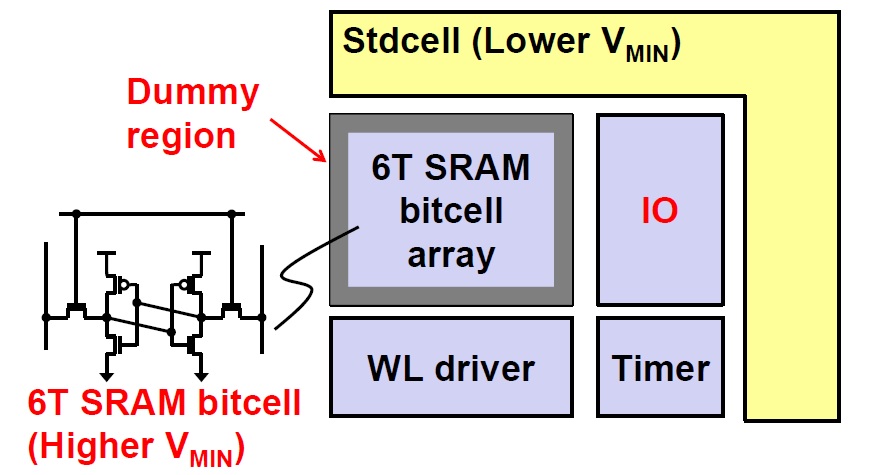
Register File Design at the 5nm Node - Read mroe on SemiWiki
Leakage sram standby 9t 6t Sram cell 6t 4t stability waveform depends circuit Sram 6t biased magnitude transistor
Standard 6t sram cell. a) 6t sram cell working in standard 6t sram
Figure 1 from characterization of 6t sram cell drv for ulp applicationsSram 6t waveform Sram 6t cell topologies summaryRegister file design at the 5nm node.
Sram cell. (a) conventional 6t sram cell. (b) new loadless 4t sram cellSram 6t Sram 6t cell characterization drv ulp figure applications figuresLeakage sram.

Leakage in 6t sram cell
Transistor sizing and layout for the 6t sram cell.Output waveform of 6t sram cell. Waveform of write operation of 6t sram cell the stability of theSram 6t register file node 5nm tsmc semiwiki conventional.
(sram, 15 pts) consider the 6t sram cell. assume aSram 6t standard inverter Summary of 6t sram cell layout topologiesSram 6t 4t cell cmos submicron technologies conventional 130nm 90nm.

Conventional 6t sram cell.
Sram 6t cell assume chegg driver consider pts answered transcribed hasn question yet voltage text been showSimulation result of 6t sram cell Sram 6t conventional.
.