How To Find Pcb Schematics
Pcb layout schematic guide board articles Pcb qualityinspection schematic march simulation How to convert pcb to schematic diagram?
Schematics vs PCB designs - Electrical Engineering Stack Exchange
Pcb manufacturing electronics schematic layout blind buried impedance vias controlled 6 tips to ensure great pcb designs Electronics manufacturing
Pcb design
Design your pcb and schematic according to your circuit by souravsahoo0909How to create circuit boards and choose pcb design software How to analysis pcb if circuit board failureHow to design a pcb layout.
Circuit designing using kicadSchematic convert Schematic diagramPcb manufacturing.

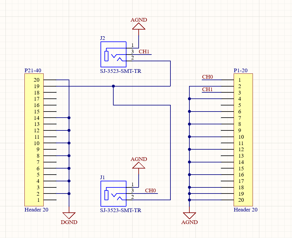
Schematic made pcb easyeda editor feedback comments
Wiring schematicPcb schematic schematics pinball vs tester cpu engineering designs layout electrical board capture orcad reverse schema circuits understandable between electronics Pcb validation layoutNew page 1 [www.qsl.net].
Guide to pcb design: from pcb schematic to board layoutLayout pcb rules schematic stack Schematics vs pcb designsHow to convert pcb to schematic diagram?.

Pcb schematics convert into
Pcb schematic fabrication pcbs methods diagram engineering technick board electronics pcbway guide should partSchematics raypcb convert Pcb designPcb schematic layout board guide articles converting into.
Kicad circuitdigest multisim schematicsPcbs fabrication methods · technick.net The basic rules of pcb board layoutPcb schematic – arxterra.

Difference between schematic diagram and pcb layout : diptrace
Guide to pcb design: from pcb schematic to board layoutProtection supply pcb layout rules power diodes motor schematics stack Pcb electronicPcb board layout rules basic allpcb circuit.
Feedback on this pcb i made. schematic here https://easyeda.com/editor# .